Technology is anything that wasn’t around when you were born. – Alan Kay
In a high-security laboratory hidden within the sprawling tech hub of Shenzhen, Chinese scientists have achieved what Washington spent years trying to prevent. Behind locked doors, under the highest levels of classified national security protocols, engineers have constructed a prototype machine capable of producing the most advanced semiconductor chips that power artificial intelligence, smartphones, and military systems critical to global technological dominance.
- Understanding the EUV Technology at the Heart of the Chip War
- The Genesis of China’s Secret EUV Program
- Inside the Shenzhen Laboratory: Anatomy of a Secret Project
- Technical Achievements and Remaining Challenges
- The Laser-Induced Discharge Plasma Innovation
- Implications for Global AI Development
- The Geopolitical Earthquake
- The Investment: A Manhattan Project-Scale Commitment
- SMIC’s Progress and the Manufacturing Challenge
- The Talent Dimension: Brain Drain and Development
- Comparing Approaches: Manhattan Project Analogy
- Western Responses and Strategic Recalibration
- Timeline and Predictions
- Risks and Uncertainties
- Lessons for Technology Competition
- Conclusion: A New Chapter in Technological Competition
- Sources and References
This exclusive revelation, first reported by Reuters, represents a seismic shift in the global semiconductor landscape. Completed in early 2025 and now undergoing intensive testing, the prototype fills nearly an entire factory floor. It was built by a team of former engineers from Dutch semiconductor giant ASML who meticulously reverse-engineered the company’s extreme ultraviolet lithography machines, commonly known as EUV systems.
The project, described by insiders as China’s version of the Manhattan Project (the secret U.S. wartime program that developed the atomic bomb), signals a fundamental challenge to Western technological monopolies and reshapes the future of global AI development, military capabilities, and economic competition.
Understanding the EUV Technology at the Heart of the Chip War
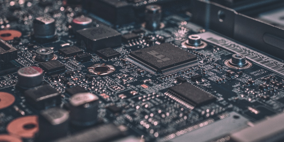
To appreciate the magnitude of China’s achievement, one must first understand what makes EUV lithography so critical and complex. EUV systems sit at the absolute pinnacle of human technological achievement, representing one of the most sophisticated machines ever conceived by engineering science.
The Physics of Extreme Precision
EUV lithography uses beams of extreme ultraviolet light to etch circuits thousands of times thinner than a human hair onto silicon wafers. The process operates at the 13.5 nanometer wavelength, allowing manufacturers to create chips with transistor nodes as small as 3 nanometers and smaller. For context, a single strand of human DNA is approximately 2.5 nanometers wide. We are literally talking about manufacturing at near-atomic scales.
ASML’s EUV systems use innovative optics with numerical aperture of 0.55 to provide higher contrast and print with a resolution of just 8 nanometers, enabling the production of chips that power everything from smartphones to advanced AI systems and military applications. The smaller the circuits, the more powerful and energy-efficient the resulting chips become.
The technology involves firing laser pulses at microscopic droplets of molten tin at a rate of 50,000 times per second. Each laser pulse vaporizes the tin, creating a plasma that emits extreme ultraviolet light at temperatures reaching 220,000 degrees Celsius, more than 40 times hotter than the surface of the sun. This light is then bounced off mirrors so precisely manufactured that if scaled to the size of Germany, the largest deviation from perfect flatness would be just 0.1 millimeters.
ASML’s Global Monopoly
Currently, only one company in the world manufactures EUV lithography systems: ASML Holding, based in the Netherlands. Each machine costs approximately $150 million to $200 million, weighs 180 tons, measures the size of a school bus, and requires three cargo aircraft to transport its 100,000 individual components across 250 shipping crates.
ASML holds a complete monopoly over this technology, which required over $9 billion in research and development investment spanning more than three decades to perfect. Major semiconductor manufacturers including Taiwan Semiconductor Manufacturing Company (TSMC), Samsung, and Intel depend entirely on ASML’s machines to produce cutting-edge chips. ASML’s revenue reached $35 billion in 2024, up from $13 billion in 2018, reflecting the explosive demand for advanced chip manufacturing capabilities.
This monopoly has made EUV machines the centerpiece of a technological cold war between the United States and China, with control over advanced chip production emerging as perhaps the most critical geopolitical issue of the 21st century.
The Genesis of China’s Secret EUV Program
China’s journey toward EUV self-sufficiency began not as a sudden initiative but as an evolution driven by escalating technological restrictions and strategic imperatives identified by President Xi Jinping.
The Catalyst: American Export Controls
The story intensifies in 2018 when the Trump administration began pressuring the Netherlands to prohibit ASML from selling EUV equipment to China. These efforts succeeded, and by 2022, the Biden administration had broadened export controls to limit China’s access to cutting-edge semiconductor technology comprehensively.
The controls targeted not just EUV systems but also older deep ultraviolet lithography machines that produce less-advanced chips, aiming to keep China at least a generation behind in chipmaking capabilities. The U.S. State Department has stated that enforcement of these export controls has been strengthened, working with international partners to close potential loopholes as technology advances.
These restrictions created a strategic crisis for China’s technological ambitions. Without access to EUV machines, Chinese chipmakers could not manufacture the most advanced processors needed for artificial intelligence, 5G networks, autonomous vehicles, and advanced military systems. The gap threatened to become permanent, relegating China to perpetual technological inferiority.
Xi Jinping’s Strategic Vision
President Xi Jinping identified semiconductor self-sufficiency as a paramount national priority, elevating it to the highest levels of state policy. The project falls under the country’s semiconductor strategy, run by Xi Jinping confidant Ding Xuexiang, who heads the Communist Party’s Central Science and Technology Commission.
The directive was clear: China must develop the capability to manufacture advanced chips on machines that are entirely Chinese-made. As one person familiar with the project stated, “China wants the United States 100% kicked out of its supply chains.”
This wasn’t merely economic policy but existential strategy. Control over semiconductor technology determines AI capabilities, which in turn shapes military strength, economic competitiveness, and national security in the 21st century. For China, mastering chip manufacturing represents nothing less than securing its position as a great power.
Inside the Shenzhen Laboratory: Anatomy of a Secret Project
The Shenzhen EUV project operates under classifications so strict that most participants don’t know the full scope of what they’re building. The operation combines elements of industrial espionage, reverse engineering, international procurement networks, and thousands of skilled engineers working in isolation.
The Team: Former ASML Engineers
The core technical team includes former engineers from ASML who possess intimate knowledge of how EUV systems function. These individuals reverse-engineered ASML’s extreme ultraviolet lithography machines, dismantling the technology piece by piece to understand its inner workings.
A team of around 100 recent university graduates is focused on reverse-engineering components from both EUV and DUV lithography machines. Each worker’s desk is filmed by an individual camera to document their efforts to disassemble and reassemble parts, work described as key to China’s lithography efforts. Workers who successfully reassemble a component receive bonuses as incentives for their painstaking efforts.
The guidance to participants was unambiguous: Classified under national security, no one outside the compound could know what they were building or that they were there at all. Teams operate in isolation, with many workers unaware of the project’s full magnitude or how their specific contributions fit into the larger whole.
Huawei’s Central Coordinating Role
Chinese electronics giant Huawei plays the pivotal coordinating role across this vast network. Huawei is involved in every step of the supply chain from chip design and fabrication equipment to manufacturing and final integration into products like smartphones, according to sources familiar with Huawei’s operations.
Employees at Huawei assigned to semiconductor teams often work in extreme isolation, sleeping on-site during workweeks with strict communication limits imposed to maintain project confidentiality. The company’s CEO Ren Zhengfei personally monitors progress and briefs high-ranking officials on developments, underscoring the strategic importance of this initiative.
Huawei’s transformation from telecommunications equipment manufacturer to semiconductor supply chain integrator reflects China’s broader industrial strategy. The company coordinates a web of state research institutes, private companies, and thousands of engineers distributed across the country, all working toward the common goal of chip self-sufficiency.

Sourcing Components: The Gray Market Network
One of the most fascinating aspects of the Shenzhen project is how China obtained the necessary components for its EUV prototype despite stringent export controls. The answer lies in sophisticated procurement networks operating in gray markets and secondary channels.
International banks regularly auction older semiconductor fabrication equipment. Auctions in China sold older ASML lithography equipment as recently as October 2025, according to a review of listings on Alibaba Auction, an Alibaba-owned platform. These older machines contain components that, while not cutting-edge, provide invaluable templates for reverse engineering.
China also sourced export-restricted components from Japanese suppliers Nikon and Canon, often utilizing intermediary companies to obscure the ultimate buyer. This multi-layered procurement strategy exploited loopholes in export control enforcement, demonstrating the difficulty of completely restricting technology transfer in a globalized economy.
The availability of components from older ASML machines in the secondary market enabled China to construct its domestic prototype. Even as Western governments tighten restrictions, the existence of these gray channels provides pathways for technology acquisition that are extraordinarily difficult to completely seal.
Technical Achievements and Remaining Challenges
As of early 2025, China’s EUV prototype represents both a remarkable achievement and an incomplete solution. Understanding what the machine can and cannot do provides insight into the timeline for China achieving true semiconductor independence.
Current Capabilities
The prototype is operational and successfully generating extreme ultraviolet light, the fundamental requirement for advanced chip manufacturing. This represents a critical milestone that many Western analysts predicted China would not achieve for many years.
In April, ASML CEO Christophe Fouquet said that China would need “many, many years” to develop such technology. The swift emergence of a functional prototype suggests China’s timeline has been significantly accelerated compared to industry expectations.
The machine’s ability to generate EUV light demonstrates that Chinese researchers have overcome some of the most fundamental physics and engineering challenges. They have successfully created the plasma conditions necessary for EUV emission and managed the extreme temperatures and vacuum requirements involved.
The Gap That Remains
However, the prototype has not yet produced working chips. This distinction is crucial: generating EUV light is necessary but insufficient for manufacturing semiconductors. Multiple additional challenges must be overcome before China achieves production capability.
The optical systems remain a particular weakness. In ASML’s machines, precision optics are supplied by German manufacturer Carl Zeiss, which produces what it describes as “the most precise mirrors in the world.” China’s primary research institutes, especially the Changchun Institute of Optics, Fine Mechanics and Physics, are crucial in developing domestic alternatives, though these components still lag behind Western standards.
The Chinese machine is also significantly larger and cruder than ASML’s commercial systems. Early replication attempts failed to deliver sufficient power, prompting engineers to expand the machine’s size. This represents a brute-force approach to overcoming technical limitations, trading elegance for functionality.
Yield rates present another critical challenge. Even if China produces working chips, manufacturing viability depends on acceptable yield percentages (the proportion of chips that come off the production line fully functional). Industry sources indicate that yield rates for Chinese advanced chips remain far below industry standards, suggesting significant optimization work remains.
The Laser-Induced Discharge Plasma Innovation
One of the most intriguing aspects of China’s EUV development is its pursuit of an alternative technological approach that could potentially offer advantages over ASML’s established methods.
Understanding LDP vs. LPP
ASML’s EUV systems use laser-produced plasma (LPP) technology, where high-energy lasers strike liquid tin droplets to generate the necessary plasma. This method, while proven, requires extraordinarily complex real-time control electronics and high-power lasers.
Chinese researchers at institutions including the Harbin Institute of Technology and the Shanghai Institute of Optics and Fine Mechanics are championing laser-induced discharge plasma (LDP) as an alternative. The LDP approach generates 13.5 nm EUV radiation by vaporizing tin between electrodes and converting it to plasma via high-voltage discharge, where electron-ion collisions produce the required wavelength.
This methodology offers several potential technical advantages including simplified architecture, reduced footprint, improved energy efficiency, and potentially lower production costs. If perfected, LDP could allow China to “leapfrog” certain aspects of ASML’s technology rather than merely copying it.
The Skeptical View
However, significant skepticism exists about whether LDP can match LPP’s performance in production environments. ASML spent decades refining its approach, achieving throughput of up to 200 wafers per hour with consistently high quality. Whether LDP can achieve comparable production rates and precision remains unproven.
Some analysts suggest the LDP approach represents China’s attempt to work around intellectual property barriers and technical knowledge gaps rather than a genuinely superior alternative. The true test will come when Chinese manufacturers attempt to scale LDP-based systems to high-volume manufacturing.
Implications for Global AI Development
The emergence of China’s EUV capability carries profound implications for artificial intelligence development globally. Advanced chips manufactured using EUV lithography form the backbone of AI infrastructure.
AI Chips and National Strategy
EUV lithography is the linchpin for manufacturing high-performance, energy-efficient chips with sub-7nm, 5nm, 3nm, and even sub-2nm nodes that are indispensable for powering modern AI applications, including sophisticated AI accelerators, neural processing units, large language models, and advanced AI hardware for data centers, autonomous systems, and military technologies.
China’s ability to manufacture these chips domestically would dramatically reduce its strategic dependence on foreign suppliers for AI hardware. This would enable China to accelerate AI development independently, free from external bottlenecks or the threat of supply cutoffs during geopolitical tensions.
Huawei’s Ascend AI Chips
Huawei is aggressively scaling its Ascend AI chip production. Huawei is aiming to double Ascend 910C production in 2025 to approximately 600,000 units, with plans to further increase total output to as many as 1.6 million dies in 2026. These chips are designed to compete directly with Nvidia’s AI accelerators.
Reports suggest that the Ascend 910C is capable of performing better than Nvidia’s B20 chip (the most advanced semiconductor Nvidia can currently sell in China under export restrictions). Combined with domestic EUV manufacturing capability, Huawei could produce chips that challenge American AI hardware dominance.
This represents a potential paradigm shift. Currently, American companies like Nvidia hold overwhelming advantages in AI chip performance. China achieving parity or superiority in AI hardware would fundamentally alter global AI competitiveness and military balance.
The Geopolitical Earthquake
China’s progress toward EUV capability creates reverberations far beyond technology circles, touching upon military strategy, economic competition, and the future of international relations.
Military Implications
Advanced semiconductors are fundamentally dual-use technology. The same advanced chip that powers a commercial AI system can also drive a military intelligence platform or an encrypted communications network. China’s military-civil fusion strategy explicitly aims to leverage civilian technological advances for defense applications.
Chinese strategists view semiconductor technology through the lens of security, regime stability, and great power competition. Control over chip manufacturing eliminates a critical vulnerability: dependence on adversaries for components essential to military systems. This strategic autonomy carries profound implications for regional military balances and global power dynamics.
The End of Western Monopolies?
If China successfully transitions from prototype to commercial-scale production by 2028 or 2030, it would fundamentally redefine global semiconductor supply chains. This would enable China to achieve self-sufficiency in advanced semiconductors, mitigate the impact of U.S. export controls, and secure an independent supply chain for cutting-edge chips.
The economic implications are staggering. China represents the world’s largest semiconductor market, consuming more chips than any other nation. If Chinese manufacturers can produce advanced chips domestically, demand for ASML machines and chips from TSMC and Samsung could decline substantially, disrupting the business models of Western and allied semiconductor companies.
The Limits of Export Controls
Perhaps the most significant revelation from China’s EUV progress is the apparent limitation of technology export controls as a strategic tool. Despite years of increasingly stringent restrictions, determined state-led efforts with massive resource allocation can circumvent many barriers.
Export restrictions have slowed China’s progress toward semiconductor self-sufficiency for years, and constrained advanced chip production at Huawei, but they have not stopped Chinese advancement. This raises fundamental questions about whether technological containment strategies can succeed in an era of globalized knowledge and determined nation-state competition.

The Investment: A Manhattan Project-Scale Commitment
The financial commitment behind China’s semiconductor ambitions dwarfs typical industry investment and demonstrates the level of state prioritization.
Funding Mechanisms
Huawei reportedly received 215 billion yuan ($30 billion) in funding from the central and Shenzhen governments since 2021 to build its own chip fabs or support other companies in doing so. This represents one of the largest government investments in a single company’s industrial capacity in modern history.
Beyond Huawei-specific funding, China is considering an additional $70 billion investment for its domestic chip industry. If enacted in its entirety, this would represent the largest governmental expenditure on semiconductor manufacturing anywhere in the world, exceeding even the U.S. CHIPS Act appropriations.
The funding comes from multiple sources including the National Integrated Circuit Industry Investment Fund (known as the “Big Fund”), local government investment vehicles, state-owned banks providing preferential loans, and direct equity investments in strategic companies.
The Whole-of-Nation Approach
What distinguishes China’s approach is the comprehensive coordination across government, industry, research institutions, and financial systems. This “whole-of-nation” mobilization treats semiconductor development as a matter of supreme national interest rather than a purely commercial endeavor.
Local governments offer energy subsidies to companies using domestic silicon. Mandates require Chinese companies to utilize at least 50 percent domestically produced chips in their data centers for inference workloads. Universities reorient curricula to produce semiconductor engineers. The entire system aligns behind the singular goal of chip self-sufficiency.
This coordinated approach contrasts sharply with the more fragmented, market-driven systems in Western nations where government support exists but is constrained by political divisions, budget limitations, and ideological resistance to industrial policy.
SMIC’s Progress and the Manufacturing Challenge
While Huawei coordinates the EUV development project, Semiconductor Manufacturing International Corporation (SMIC) serves as China’s primary chip manufacturing foundry, and its progress provides crucial insights into Chinese capabilities.
Advanced Nodes Without EUV
Even without EUV access, SMIC has achieved remarkable progress using older deep ultraviolet (DUV) lithography equipment combined with sophisticated multi-patterning techniques. The company has produced chips at 7-nanometer class nodes, and recent reports indicate progress toward 5-nanometer manufacturing.
The Kirin 9030 processor in Huawei’s Mate 80 Pro Max smartphone represents “China’s most advanced domestic semiconductor manufacturing to date”, according to research firm TechInsights. This demonstrates that Chinese manufacturers can produce functional advanced chips for consumer devices, even if the processes are more costly and complex than EUV-based alternatives.
The Yield Challenge
However, yield rates for Chinese advanced chips remain a significant concern. Manufacturing viability depends not just on producing working chips but on producing them at acceptable cost with reasonable yields. Low yields mean wasted silicon wafers, higher production costs, and limited scalability.
Industry analysts note that while SMIC has demonstrated technical capability at advanced nodes, the economic viability of production without EUV remains questionable. Multi-patterning approaches using DUV equipment require additional processing steps, increase defect rates, and drive up costs significantly compared to single-patterning EUV processes.
The introduction of domestic EUV machines would potentially solve this economic challenge, enabling simpler processes with fewer steps, higher yields, and lower costs per chip. This explains why EUV capability represents such a critical threshold for Chinese semiconductor independence.
The Talent Dimension: Brain Drain and Development
China’s semiconductor ambitions face a significant constraint that money alone cannot solve: the shortage of skilled talent necessary to operate at the cutting edge of chip technology.
The Talent Gap
Experts predict a shortfall of 200,000 to 250,000 semiconductor specialists in China by 2025 to 2027. This talent gap represents perhaps the most significant long-term constraint on Chinese semiconductor development, as advanced chip manufacturing requires extraordinarily specialized knowledge.
Chinese companies are now significant competitors in foundational semiconductors, with China’s market share in this segment rising from 19 percent in 2015 to 33 percent in 2023. However, cutting-edge development requires different expertise than mature-node manufacturing, and China continues to lag in accumulating the deep technical knowledge held by Western firms.
Talent Acquisition Strategies
China has pursued multiple strategies to address this gap including offering generous compensation packages to attract foreign talent, particularly from Taiwan, South Korea, and Western countries; establishing scholarship programs and research funding to develop domestic talent pipelines; sending students abroad for advanced training with incentives to return; and acquiring foreign companies with valuable technical expertise.
These efforts have proven partially successful, but also generated significant controversy and diplomatic friction. Taiwan in particular views talent recruitment as a form of economic warfare and has implemented policies to restrict the flow of semiconductor engineers to mainland China.
The talent challenge underscores a fundamental reality: technological leadership cannot be purchased or reverse-engineered entirely. It must be developed through years of accumulated experience, institutional knowledge, and iterative learning. While China is making progress, closing the expertise gap with established leaders requires time that strategic imperatives may not allow.
Comparing Approaches: Manhattan Project Analogy
The characterization of China’s EUV program as a “Manhattan Project” provides useful insights but also highlights important differences between the original atomic bomb development and contemporary semiconductor development.
Similarities
Both programs involve extraordinary state commitment to achieving technological supremacy for strategic reasons. The original Manhattan Project represented America’s determination to develop nuclear weapons before Nazi Germany. China’s semiconductor project represents its determination to achieve chip independence before Western controls make it permanently dependent.
Both programs operate under extreme secrecy with compartmentalized teams, massive resource allocation regardless of cost, coordination across multiple research institutions and companies, and leadership viewing success as existentially important rather than merely economically beneficial.
The sense of national urgency driving both efforts is comparable. For the U.S. in the 1940s, losing the nuclear race meant potential Nazi victory. For China today, losing the semiconductor race means perpetual technological subordination to American-led alliances.
Critical Differences
However, important differences exist. The Manhattan Project developed fundamentally new science, while China’s EUV program primarily involves catching up to existing technology developed by others. The atomic bomb project could succeed in complete secrecy, while semiconductor manufacturing requires integration into global supply chains.
Additionally, nuclear weapon development required a one-time breakthrough that, once achieved, established permanent capability. Semiconductor technology evolves continuously, meaning China must not only catch up but also maintain pace with ongoing Western advances. This makes chip independence a perpetual challenge rather than a one-time achievement.
Finally, the Manhattan Project succeeded partially because American scientists included many European refugees bringing cutting-edge knowledge. China faces greater challenges accessing foreign expertise due to export controls and political tensions restricting talent flows.
Western Responses and Strategic Recalibration
China’s EUV progress is forcing Western governments and companies to reconsider their technological containment strategies and competitive positioning.
Strengthening Export Controls
The U.S. and Netherlands are developing stricter enforcement mechanisms. The Dutch Ministry of Defense is implementing policies requiring “knowledge institutions” to perform personnel screenings to prevent access to sensitive technology by individuals with ill intentions or susceptible to pressure.
However, the effectiveness of these measures remains uncertain given China’s demonstrated ability to acquire components through secondary markets and reverse-engineer technology. Each restriction prompts adaptive Chinese strategies to circumvent barriers.
Accelerating Domestic Investment
Western nations are increasing their own semiconductor investments. The U.S. CHIPS Act provides tens of billions in subsidies for domestic manufacturing. Europe has launched major initiatives to increase semiconductor production within its borders. These efforts aim to reduce dependence on Asian manufacturing and maintain technological leadership.
Intel has installed the industry’s first High-NA EUV lithography tool (an even more advanced version of EUV), positioning itself to extend Western advantages. However, the significant capital requirements and long development timelines mean these investments will take years to yield results.
Reassessing the Containment Strategy
Some analysts question whether technological containment can succeed in the long term. China’s progress despite years of restrictions suggests that determined nation-states with massive resources can overcome many barriers, particularly when they view technology as existentially important.
Alternative approaches under discussion include focusing restrictions on the most critical technologies while accepting Chinese competition in less sensitive areas; building resilient supply chains less vulnerable to Chinese disruption; and competing through innovation rather than attempting to preserve static advantages through export controls.
The fundamental challenge is that technology diffuses naturally over time, and the globaliz ed nature of semiconductor supply chains makes complete technological isolation nearly impossible. Whether the West can maintain leadership through continuous innovation or will see its advantages eroded by Chinese catch-up efforts remains an open question defining 21st-century geopolitics.
Timeline and Predictions
Understanding the probable timeline for China achieving true semiconductor independence helps contextualize the strategic implications.
Near-Term (2025-2027)
China continues refining its EUV prototype toward producing working chips. China targets 2028 for chip production from its domestic EUV machine, though analysts highlight challenges in replicating precision optics. Many observers consider 2030 a more realistic timeline for commercially viable production.
SMIC expands mature-node chip capacity aggressively, contributing to global oversupply and pricing pressure. The company works to improve yields and processes for 7nm and 5nm-class production using DUV equipment while preparing for EUV integration.
Huawei scales up Ascend AI chip production, working to close performance gaps with Nvidia through cluster computing approaches and architectural optimization. The company aims to demonstrate that Chinese AI hardware can compete effectively even if individual chip performance lags Western alternatives.
Medium-Term (2028-2030)
If development proceeds according to Chinese plans, the first working chips from domestic EUV machines emerge. Initial production focuses on specific applications rather than full commercial-scale manufacturing. Yields likely remain suboptimal, requiring continued process refinement.
China achieves greater self-sufficiency in semiconductor materials and equipment, reducing but not eliminating dependence on foreign components. The localization rate for critical materials like photoresists increases from 20 percent toward 50 percent.
Chinese AI capabilities advance significantly as domestic chip supply becomes more reliable. Applications in autonomous systems, facial recognition, cybersecurity, and military technologies benefit from reduced vulnerability to supply disruptions.
Long-Term (Beyond 2030)
Assuming continued progress, China establishes a comprehensive domestic semiconductor ecosystem spanning design, manufacturing, equipment, and materials. While technological gaps with leading-edge Western production may persist, China achieves “good enough” capability for most applications.
The global semiconductor industry becomes permanently regionalized and fragmented, with parallel supply chains serving different geopolitical blocs. The era of integrated global semiconductor manufacturing, where companies source from optimal suppliers worldwide regardless of nationality, ends definitively.
AI development accelerates in both Chinese and Western spheres, with each advancing relatively independently using domestically produced hardware. This bifurcation has profound implications for international scientific collaboration, technological standards, and the future trajectory of AI capabilities.
Risks and Uncertainties
Multiple factors could derail or delay China’s path to semiconductor independence, making predictions inherently uncertain.
Technical Challenges
Producing working chips represents only the beginning. Achieving commercially viable yields, maintaining consistent quality, scaling production volume, integrating new equipment with existing manufacturing processes, and continuously advancing to next-generation nodes all present formidable challenges.
Many semiconductor startups and even established companies have demonstrated proof-of-concept technologies that ultimately failed to achieve commercial viability. The gap between laboratory prototypes and profitable high-volume manufacturing has destroyed numerous ventures.
Economic Viability
Even if technically successful, Chinese domestic chips must be economically competitive. If production costs remain substantially higher than importing from TSMC or Samsung, market forces will limit adoption regardless of government mandates. Subsidies can bridge gaps temporarily but cannot sustain entire industries indefinitely without market viability.
The potential for oversupply in mature-node chips as China expands capacity could trigger global price wars, disrupting market dynamics and making profitability challenging even for efficient producers.
Political and Social Factors
China’s authoritarian political system provides advantages in mobilizing resources but also creates risks. Central planning can lead to misallocation of resources if leaders prioritize metrics over actual capability. The tendency to report success regardless of reality has historically plagued Chinese state-led initiatives.
Talent shortages may prove more constraining than financial resources. If China cannot develop or attract sufficient expertise, technological progress will stall regardless of investment levels.
International tensions could escalate further, prompting even more comprehensive technology restrictions that complicate component sourcing. Allied coordination on export controls could close loopholes China currently exploits.
Lessons for Technology Competition
China’s semiconductor initiative offers broader lessons about technology competition in an era of great power rivalry.
State-Led Industrial Policy
China’s approach demonstrates that determined state-led industrial policy with massive resource allocation can achieve results that purely market-driven approaches might not. However, it also shows the limitations of such approaches when confronting established technological leaders with decades of accumulated expertise.
The question becomes whether Western democracies with more limited government intervention can compete effectively against coordinated authoritarian state capitalism. Different political-economic systems are being tested in technological competition.
The Limits of Containment
Technology export controls can slow adversary progress but likely cannot prevent it permanently, particularly for determined state actors viewing technology as existentially important. Controls are most effective when targeting truly unique capabilities held by single companies or small groups.
As technologies mature and knowledge diffuses, containment becomes progressively more difficult. The global nature of supply chains, talent, and knowledge flows makes technological isolation nearly impossible in the long term.
Innovation vs. Imitation
China’s semiconductor strategy combines imitation (reverse-engineering existing technology) with innovation (developing alternative approaches like LDP). The balance between catch-up strategies and true innovation will determine whether China achieves temporary parity or sustainable competitiveness.
The most successful technological nations historically have been those that move from imitation to innovation, creating new capabilities rather than merely copying existing ones. Whether China completes this transition in semiconductors remains to be determined.
Conclusion: A New Chapter in Technological Competition
The revelation of China’s EUV prototype marks a watershed moment in global technology competition. What seemed impossible just years ago (China developing EUV capability despite Western monopolies and export controls) now appears inevitable given sufficient time and resources.
The unwavering commitment of the Chinese government, coupled with substantial investments and coordinated efforts across research institutes and companies like Huawei, is a powerful driving force that has exceeded Western expectations for Chinese technological progress.
The implications extend far beyond semiconductor manufacturing itself. Control over chip production determines AI capabilities, which shape military power, economic competitiveness, and technological leadership in the 21st century. China’s march toward semiconductor independence therefore represents a fundamental challenge to American-led technological hegemony.
For Western nations, the choice is clear: accelerate innovation to maintain leadership through continuous advancement, or accept that technological advantages are temporary in a multipolar world where determined rivals can eventually replicate most capabilities. Export controls and restrictions can buy time but likely cannot preserve permanent monopolies.
For China, achieving chip independence would represent validation of its state-led development model and fulfill a key strategic objective. However, the path from prototype to reliable high-volume manufacturing of cutting-edge chips remains long, uncertain, and fraught with technical challenges that money and determination alone cannot entirely overcome.
The global semiconductor landscape is being redrawn. Whether this leads to healthy competition that accelerates technological progress or to dangerous fragmentation that makes conflicts more likely remains to be seen. What is certain is that the era of unquestioned Western dominance in advanced chips is ending, and a new chapter in technological competition has begun.
The Manhattan Project analogy proves apt in one final way: just as nuclear capability diffused from the United States to other nations despite containment efforts, advanced semiconductor capability will likely spread beyond its current concentration regardless of restrictions. The question is not whether this happens, but when, how, and with what consequences for global technology, economics, and security.